
Refers to the semiconductor module that integrates multiple semiconductor chips and passives in one package to achieve system-level electrical performance. ACCESS’ substrates provide a high-density layout for active and passive devices, to realize the high performance requirements of the customers design with high heat dissipation using proprietary technology that can channel heat thru the substrate and is being used by many of ACCESS’ customers.

 1.5~12 layers, odd or even layer substrates, ultra-thin substrate stack-up
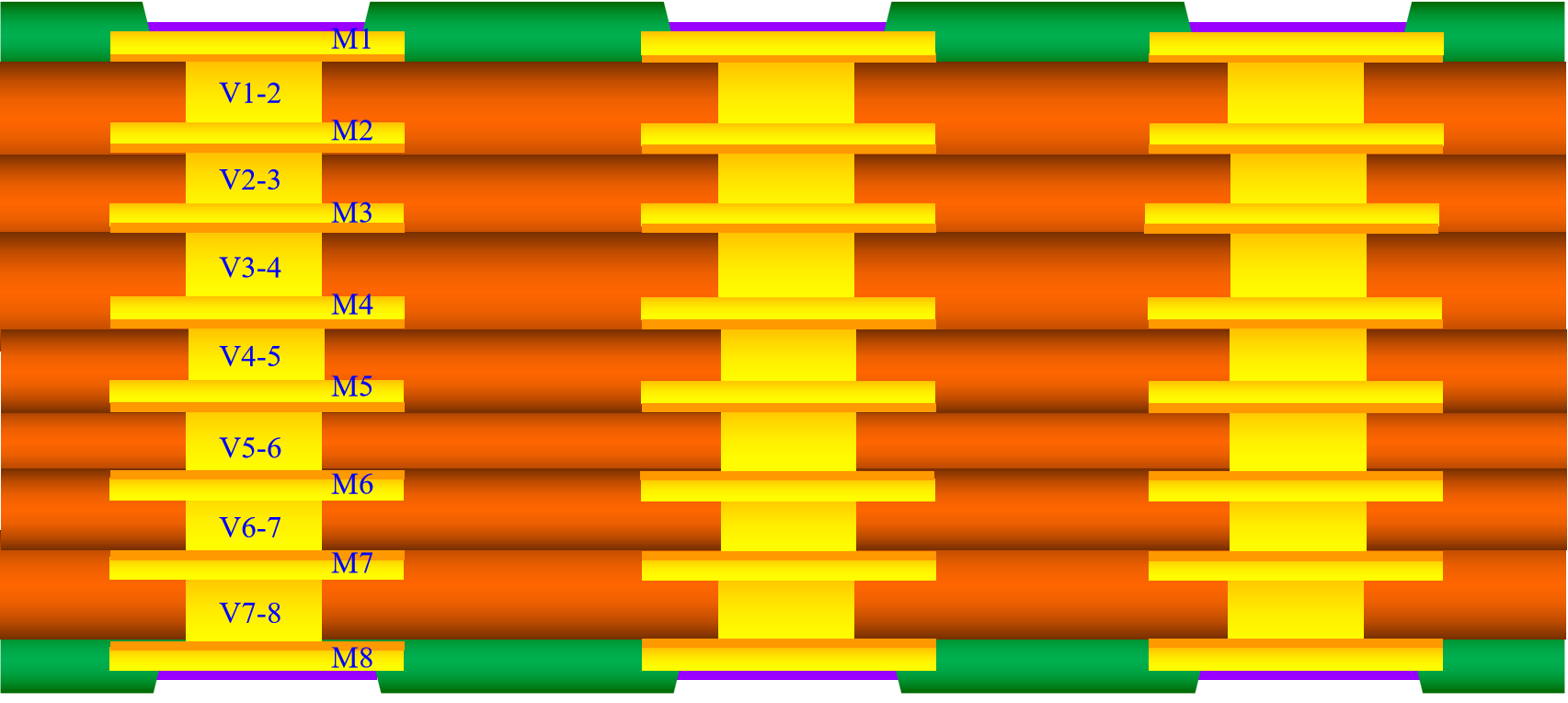
 Using via post or copper pillar instead of laser via to realize high-density interconnection of any layer and any shape
 Via Post or Copper pillar is a sequential build-up substrate plating process which can be started and interconnected at any layer
 The consistency of copper pillar interconnection can improve the performance of RF package and ensure signal integrity
 Large Copper block structures can be plated within the substrate to reduce IR drop and improve power integrity
 Stacked bar-shape copper pillars or plated heat spreaders create a three-dimensional connection channel for efficient heat dissipation for the chip
 Compatible with traditional Tenting/MSAP technology


