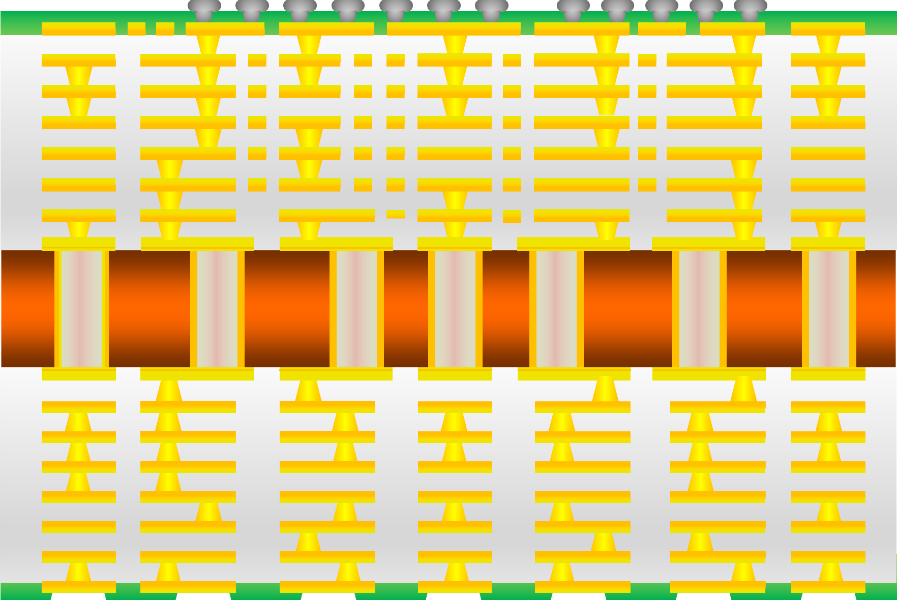

FCBGA (Flip-Chip Ball Grid Array), which is using the high-density micro bumps to connect the digital chips and substrate through the Flip Chip process, and place the passive devices next to the chips on the surface of substrate, to form BGA (Ball Grid Array) or LGA (Land Grid Array) package type. ACCESS uses SAP (Semi-additive process) technology to manufacture the FCBGA substrate with high density and high layer counts to support the high-end flip chips, and make sure the high efficiency electrical interconnect and high-speed transmission.

 4~20 layers or above stack-up to realize the high-density interconnection requirement of advanced wafer process
 To utilize SAP process to bring high precision and high density of fine lines
 High precision, high density laser micro-via technology with superior alignment capability
 uBall technology is used to place up to tens of thousands of micro Sn balls on the top surface of the substrate. These Sn balls are used for connection with the micro bump on the flip chip die surface
  Ball Grid Array (BGA) or Land Grid Array (LGA) use this technology for connectivity to the die


